June 21, 2022
Others
Development of Poly-OS, a Poly-Crystalline Oxide Semiconductor Applicable to a Wide Variety of Displays
Idemitsu Kosan Co.,Ltd.
Japan Display Inc.
Idemitsu Kosan Co., Ltd. ("Idemitsu Kosan," Head Office: Chiyoda-ku, Tokyo; President and Chief Executive Officer: Shunichi Kito), and Japan Display Inc. ("JDI," Head Office: Minato-ku, Tokyo; Chairman and Chief Executive Officer: Scott Callon) have successfully co-developed an innovative poly-crystalline oxide semiconductor, Poly-OS, for use in a wide variety of displays, including wearable devices, smartphones, metaverse devices such as VR, Notebook PCs, and large-display TVs.
By integrating Idemitsu Kosan's newly developed proprietary poly-crystalline oxide*1semiconductor material and JDI's proprietary backplane*2 technology, the new Poly-OS semiconductor contributes significantly to improving display performance by achieving both high mobility and low off-leak current*3 on Gen 6 mass production lines. Poly-OS can also be deployed to large-size Gen 8 lines and above, significantly reducing display manufacturing costs. Both JDI and Idemitsu Kosan are committed to actively promoting this innovative technology globally.
Idemitsu Kosan started the development of a poly-crystalline oxide semiconductor material IGO (Indium Gallium Oxide) for flat panel displays as part of its electronic materials business in 2006. IGO has high mobility equivalent to low temperature polysilicon (LTPS)*4, which could not be achieved with existing oxide semiconductors, along with stable thin-film transistor (TFT)*5 characteristics that can be applied to Gen 8 and larger substrate lines.
JDI has succeeded in developing the world's first practical application of Poly-OS on a Gen 6 mass production line at its Mobara Plant (Mobara City, Chiba Prefecture), using its proprietary backplane technology. JDI’s HMO (High Mobility Oxide) Poly-OS implementation achieves 4X higher field-effect mobility than conventional OS-TFTs. JDI announced this HMO technology breakthrough on March 30, 2022. (News release: "World's first oxide semiconductor TFT with four times the field-effect mobility of conventional technology realized on 6th generation mass production line"
JDI release: "JDI Develops World's First G6 Oxide Semiconductor TFT with 4X Improvement in Field-Effect Mobility – Breakthrough in Display Performance – ").
Both Idemitsu Kosan and JDI are supporting the ongoing development of Poly-OS technology so that it can be widely applied in diverse applications across the global display industry. JDI and Idemitsu Kosan are committed to contributing to a low-carbon society through display performance improvements, the evolution of the global display industry, and lower display power consumption.
- 1. Polycrystalline oxide: A thin polycrystalline film composed of metal elements and oxygen.
- 2. Backplane: A circuit board on which the tiny semiconductor elements that form the basis of a flat-panel display are mounted.
- 3. Off-leakage current: Unintentional current that leaks out when a transistor is in the off state.
- 4. Low Temperature Polysilicon (LTPS): Polycrystalline silicon formed on a glass substrate at low temperatures. High electron mobility.
- 5. Thin-film transistor (TFT): A thin transistor made of silicon or other materials mounted on a glass substrate.
About Poly-OS
Technology Overview
Like a-Si*6, conventional oxide semiconductor transistors can be easily manufactured on large areas and have low power consumption due to low off-leak current. However, their mobility is lower than that of LTPS, a high-performance technology mainly used in small- and medium-sized displays. The innovative Poly-OS semiconductor technology developed by JDI and Idemitsu Kosan significantly improves and resolves the challenges of conventional oxide’s low field-effect mobility, while enabling higher performance equivalent to LTPS. Poly-OS thus makes it possible to create products that bring together the best features of existing backplane technologies (Fig. 1).
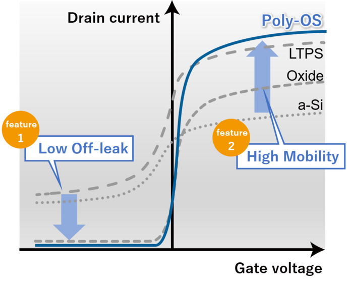
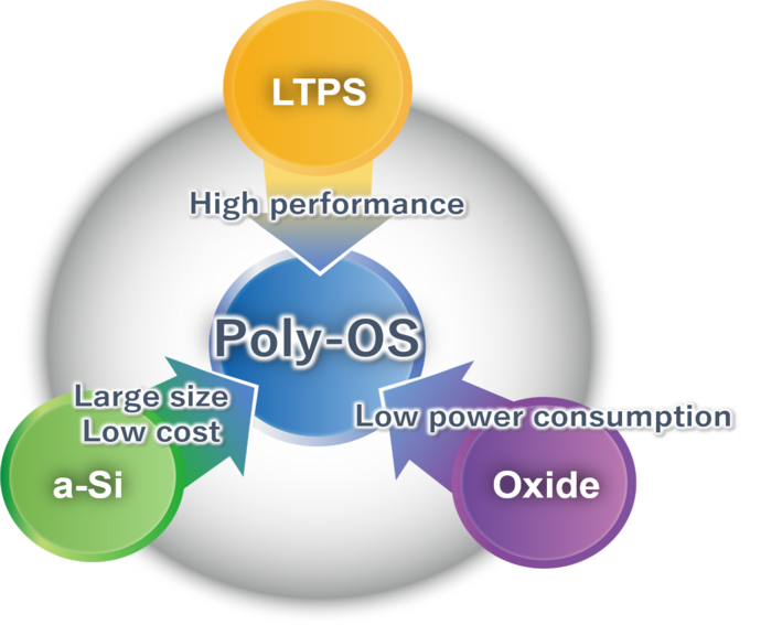
Fig. 1 Technology concept
Classification of Oxide Semiconductors
Oxide semiconductors with structures such as amorphous and C-axis aligned crystal/nano crystal*7 have been used in the active layer of transistors and thus are well-established and commercialized as mass production technologies. Idemitsu Kosan’s proprietary IGO is characterized by its ability to generate a poly-crystalline state (Fig. 2) using the conventional process (450°C or lower) similar to existing amorphous oxide semiconductors. By using this poly-crystalline oxide semiconductor in the active layer, it is possible to maximize the inherent electron mobility of oxides.
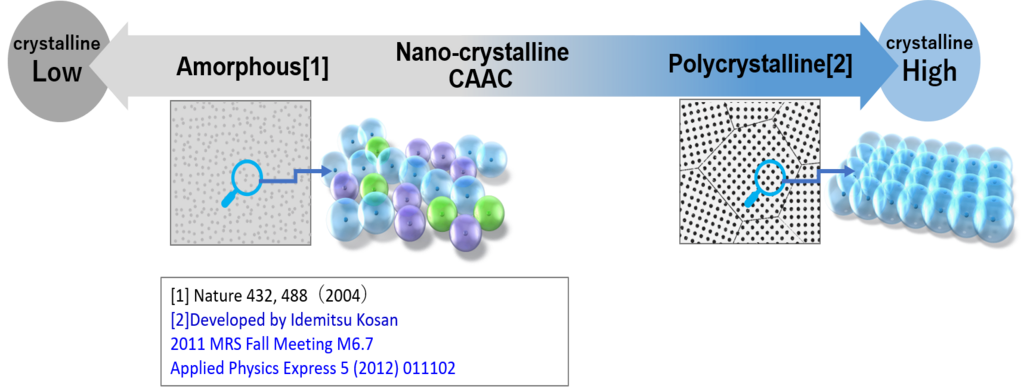
Fig. 2 Crystallinity of oxide semiconductors
Process Technology
Oxide materials with high electron mobility typically have difficulty controlling charge carriers and cannot be operated as transistors without modification. By integrating JDI’s proven process know-how in CVD*8, sputter*9, annealing*10, and etching, Poly-OS makes possible stable operation with both high mobility and low off-leak current (Fig. 3 & 4). In addition, by adopting an optimal top-gate self-align structure*11 (Fig. 5) to increase on-current*12, stable characteristics that are independent of the channel width can be obtained even at 2 µm (the minimum channel length). The current driving capability is also equivalent to that of LTPS (Fig. 6).
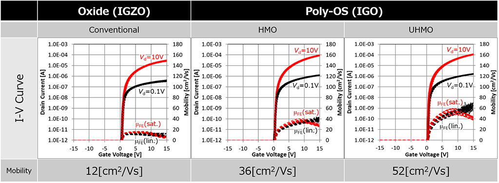
Fig. 3 Comparison of voltage-current characteristics of thin-film transistors with the same structure on a Gen 6 mass production line
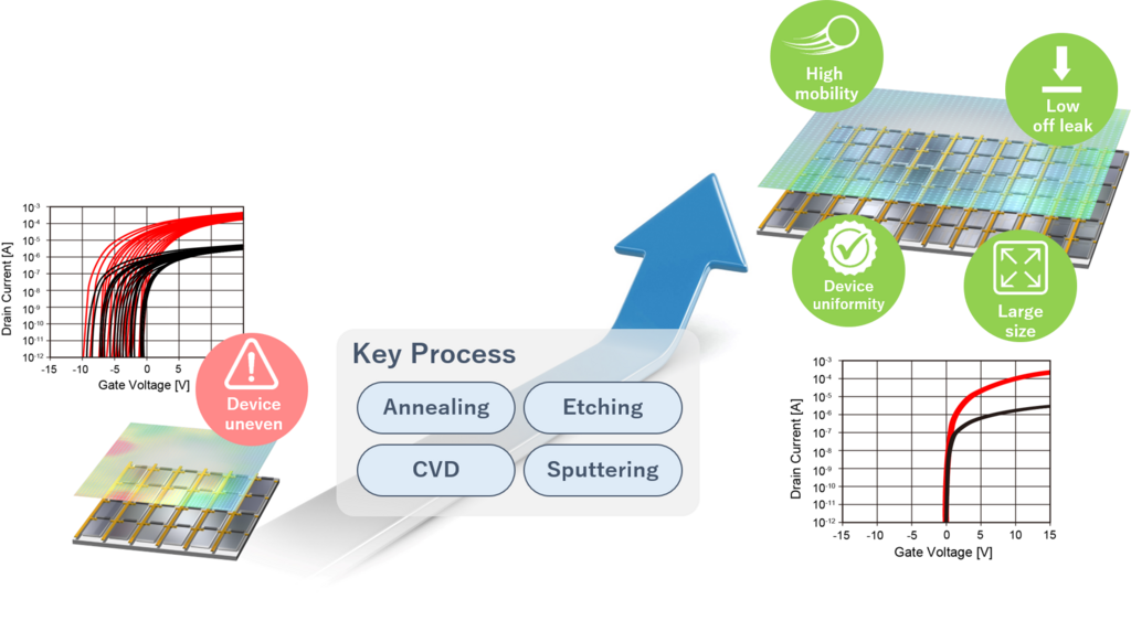
Fig. 4 Improvement of uniformity on a Gen 6 mother glass*13 (N=28pt)
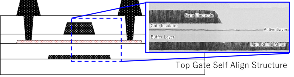
Fig. 5 Cross-sectional structure of a thin-film transistor
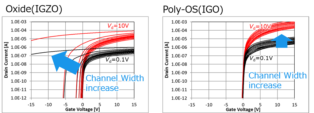
Fig. 6 Current increase when channel width in TFT is changed from 2 μm to 25 μm with a channel length of 2 μm
- 6. Amorphous Silicon (a-Si): Non-crystalline silicon used in thin film transistors.
- 7. C-axis Aligned Crystal/nano crystal: Crystal structure of a semiconductor film with c-axis alignment or nanocrystals.
- 8. CVD: A process in which a thin film is formed on a substrate surface through a chemical reaction.
- 9. Sputtering: The process of forming a thin film by bombarding a target (thin film material) with ions.
- 10. Annealing: A processing process in which heat is applied to thin films on glass substrates to improve film quality.
- 11. On-state current: The current that flows when a transistor is on.
- 12. Top Gate Self Align Structure: A TFT structure that reduces parasitic capacitance and enables high-speed operation.
- 13. Mother glass: Large-sized glass used as the glass substrate for flat-screen displays.
Company Profiles
| Name | Idemitsu Kosan Co.,Ltd. |
|---|---|
| Location | 2-1, Otemachi 1-chome, Chiyoda-ku, Tokyo |
| Representative | Shunichi Kito, Representative Director, President & Chief Executive Officer |
| Established | 1940 (founded in 1911) |
| Capital | 168.3 billion yen |
| Sales | 6.7 trillion yen |
| Name | Japan Display Inc. (JDI) |
|---|---|
| Location | 7-1, Nishi-shinbashi 3-chome, Minato-ku, Tokyo |
| Representative | Representative Executive Officer, Chairman, and Chief Executive Officer Scott Callon |
| Business Start | 2012 |
| Capital | 100 million yen |
| Sales | 295.9 billion yen |
[Contact information]
Idemitsu Kosan Co., Ltd. PR Section, Public Relations Department https://www.idemitsu.com/en/contact/flow/index.html
JDI Corporate Communication Department https://www.j-display.com/contact.html https://www.j-display.com/en/contact.html
Regarding news release
contact information
Idemitsu Kosan Co.,Ltd. Public Relations Department, Public Relations Division